Pages · 1/6
Five names, one easily misread event
On 20 October, a joint proposal by LSTC (the Leading-edge Semiconductor Technology Center), Hokkaido University, Fujifilm, GE HealthCare and imec was selected by NEDO, under a theme with "2nm" in its name. Be clear first: building a chip is not in this project's scope. It builds AI systems, optimises models for inference chips, and validates them in a hospital. Who designs the chip, and who makes it, is undecided today.
Pages · 2/6
Why a hospital
GPUs hit three walls in hospitals.
- Fit: a high-performance GPU draws 300–700 watts (the briefing's figure) — heat and bulk that are hard to build into medical equipment.
- Exit: patient data is sensitive, and sending it to an outside cloud is awkward on bandwidth, latency and compliance.
- Speed: a current GPU running several AI models over 4K surgical video drops to 1–2 frames a second.
What a hospital lacks is not peak compute. It is compute that can enter the room.
Pages · 3/6
Three systems, three sets of numbers
These numbers come from the adoption briefing. Reports that repeat them as results have misread them.
Pages · 4/6
Homework first, chip later
Work starts in September 2026: training and algorithm development on GPUs, inference on IBM's Spyre accelerator (made by Samsung on 5nm). March 2029 is the stage gate — and what is due there is not a chip. It is a quantitative forecast, built from measured data, of whether moving to 2nm can deliver 5x the speed and 10x the efficiency. Only after passing does the project move to validation on actual 2nm silicon, ending in September 2031. Device certification and market launch come after that.
Pages · 5/6
Who makes it is undecided
Professor Yosuke Kudo told the Nikkei the "leading candidate is Rapidus". The briefing line (TECH+) is cooler: LSTC hopes for a domestic chip, Rapidus manufacturing is "one of the candidates", the chip is envisaged as designed by IBM, and neither designer nor manufacturer is fixed. Both statements are true; the temperatures differ. The one checkpoint that matters most is March 2029.
Pages · 6/6
This project builds no chip. Its scope stops at three things: AI models, the optimisation that moves those models onto inference silicon, and validation of usefulness in a hospital — the development of the semiconductor device itself is not included. The more than ¥6bn spent before the stage gate buys a requirements specification written in measured clinical data, and a review in March 2029. As for the 2nm chip in the title: it is envisaged as designed by IBM, its manufacturer is undecided — and for the project's first two and a half years, it will not exist as hardware.
A NEDO medical-AI project led by LSTC will not build a chip: its scope stops at AI models, optimisation and clinical validation. Over ¥6bn before a March 2029 gate buys a requirements spec written in hospital data. Who designs or makes the 2nm chip is undecided.
Key takeaways
- Money and rules first: the pre-gate budget is over ¥6bn and the project runs September 2026 to September 2031; NEDO received exactly one proposal for this theme, and selected it.
- The targets are now concrete: CT reconstruction 5→25 slices a second; segmentation of some 1,000 anatomical classes from ~25 seconds to within 5; ultrasound overlay at 15 frames a second; 4K surgical video from 1–2 to 30 frames. Together with ≥5x speed and ≥10x efficiency, all are targets. None is measured.
- The chip is doubly undecided: envisaged as designed by IBM, manufacturer open. Kudo calls Rapidus the "leading candidate" (Nikkei); the briefing line is only "one of the candidates" (TECH+). The sources differ in temperature.
- There is one hinge date: the stage gate in March 2029. Actual 2nm silicon comes only after passing it; device certification follows the project's end in September 2031, and market launch after that.
This project builds no chip. Its scope stops at three things: AI models, the optimisation that moves those models onto inference silicon, and validation of usefulness in a hospital — the development of the semiconductor device itself is not included. The more than ¥6bn spent before the stage gate buys a requirements specification written in measured clinical data, and a review in March 2029. As for the 2nm chip in the title: it is envisaged as designed by IBM, its manufacturer is undecided — and for the project's first two and a half years, it will not exist as hardware.
In a hospital, the GPU hits three walls
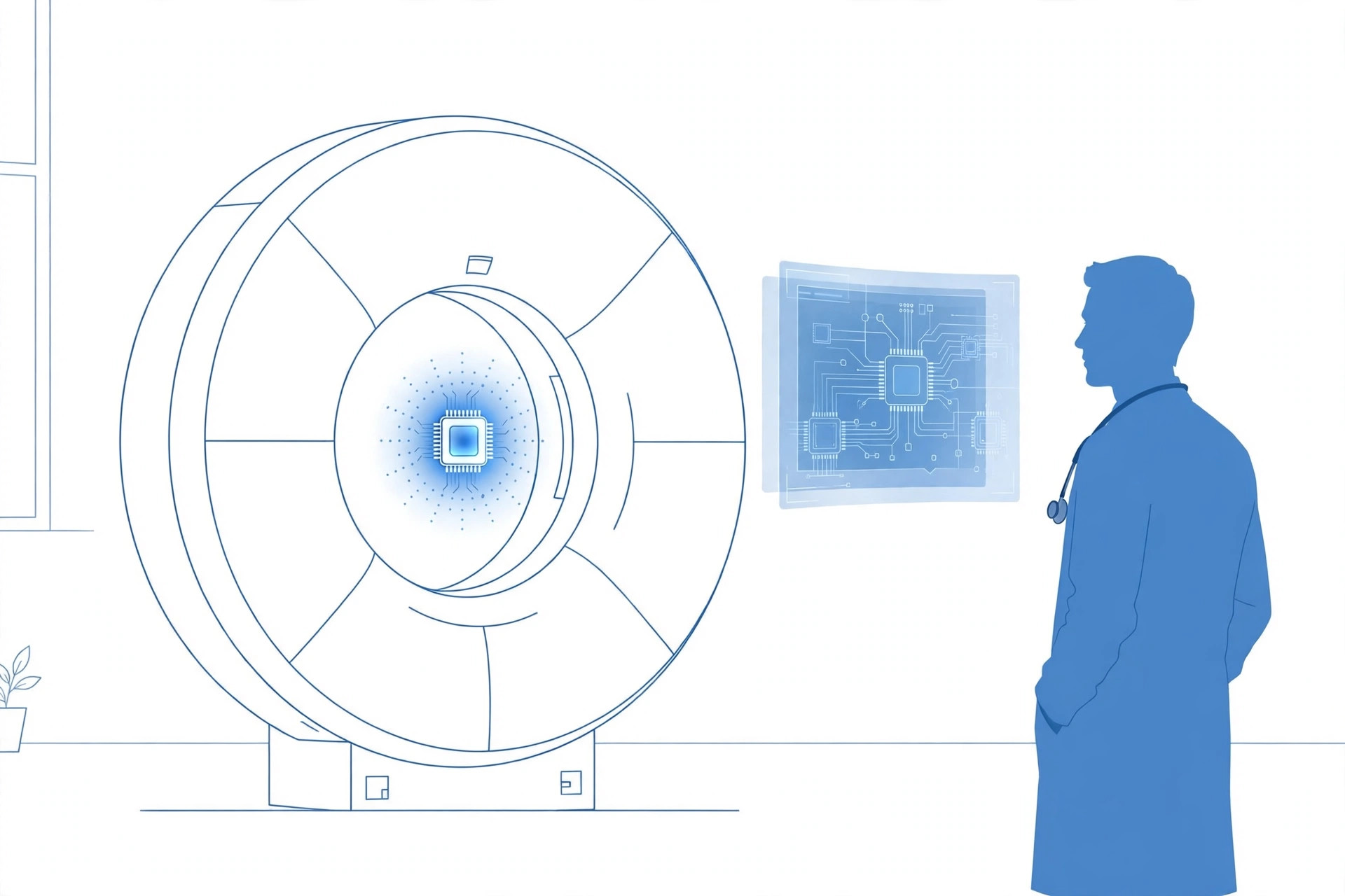
Start with the problem. CT, MRI, ultrasound and surgical microscopes produce ever higher-resolution images, and the data swells with them — above all photon-counting CT, the next-generation scanner that counts individual X-ray photons and measures their energy, and the subject of this project's first system. The briefing's figures: resolution can rise to about four times the conventional level, and material-decomposition information multiplies the data volume a further three to five times. The natural tool for such data is a GPU, but a high-performance GPU draws 300–700 watts. In a data centre that is unremarkable. In a machine that must fit an examination room or be wheeled to an operating table, heat, volume and power supply are hard constraints.
The second wall is where the data sits. Patient information is sensitive; processing it in an outside cloud is awkward on bandwidth, latency and compliance. The project's own phrasing is "hard to send out", not "cannot be sent out" — the distinction matters. The third wall has a concrete shape. Clinical work runs trained models for inference — judging "what is this" — and does not need everything a general-purpose GPU carries for large-scale training. What it needs is the answer immediately. A current GPU running several AI processes at once over 4K surgical video falls to 1–2 frames a second (briefing figure).
That is why the technical choice is written into the theme's name from the start: inference-specific. Not a general compute giant, but a chip that only infers — fast, and cool enough to live inside the equipment.
Three systems, three rooms
Real-time image diagnosis support (Hokkaido University + Fujifilm). High-speed reconstruction AI and organ-segmentation AI for photon-counting CT: reconstruction from 5 slices a second to 25; segmentation of some 1,000 anatomical classes across the body from about 25 seconds to within 5, supporting radiologists' reading and reporting. Fujifilm's aim goes beyond the AI — system development aimed at CT scanners, PACS (imaging systems) and reading terminals (press release). The chip, in other words, is a ticket in; the product is the workflow of the whole device.
Real-time clinical support (Hokkaido University + GE HealthCare). Live ultrasound images overlaid in real time on previously acquired CT or MRI scans, continuously correcting for organs that move and deform with breathing, at a target of 15 frames a second. The envisaged settings are heat ablation of liver tumours and needle biopsies (briefing).
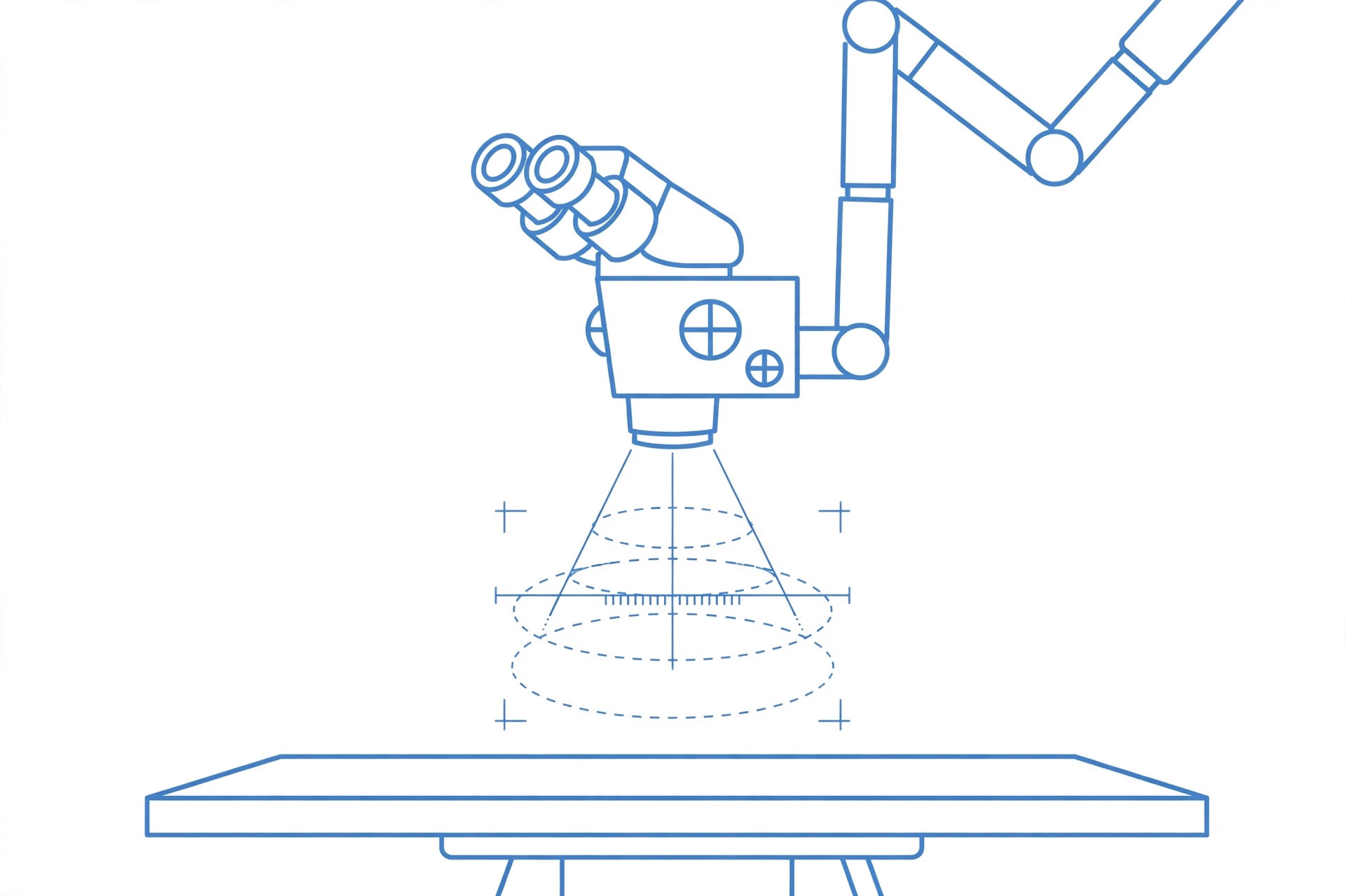
Real-time surgical support (Hokkaido University, with imec supporting). Building on the university's existing neurosurgical video AI, three processes — instrument tracking, anatomical-structure recognition, bleeding detection — are integrated into a small "AI Box" that can sit in an operating room: from the current 1–2 frames a second at 4K to 30. imec's part is to convert the models, quantise them, and integrate them into the inference chip's pipeline.
All three systems share one foundation: an inference platform running in real time inside the machine, at the edge.
Homework first, chip later
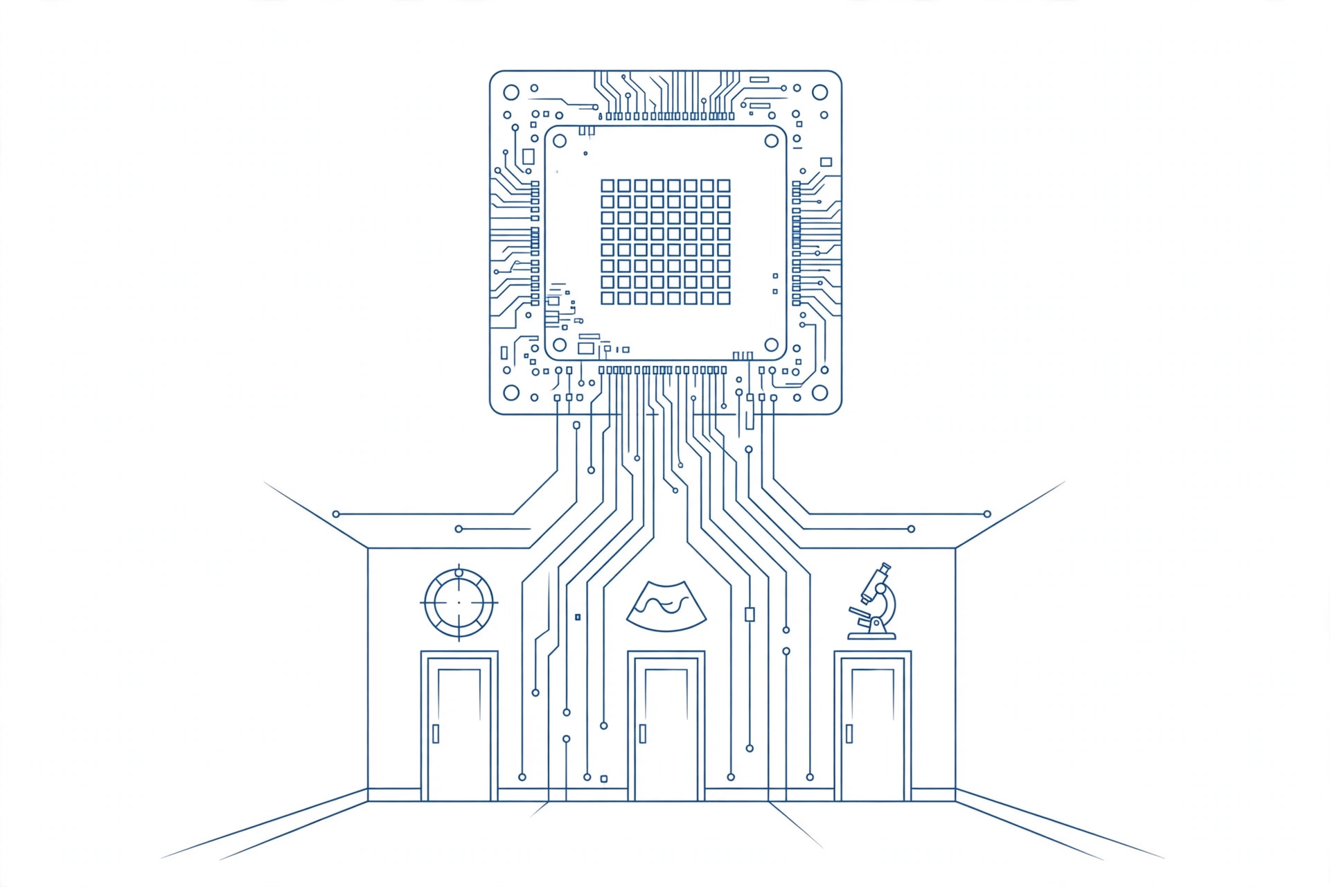
The most instructive thing about this project is its sequence. In the first phase, up to the stage gate in March 2029, model training and algorithm development proceed in a GPU environment while inference runs on IBM's Spyre — an accelerator fabricated by Samsung on 5nm, chosen because its development environment and architecture have high affinity with the envisaged 2nm chip (briefing). Two deliverables are due before the gate: the three systems implemented, functionally verified and optimised on Spyre; and a quantitative forecast — grounded in measured values, showing that migrating to 2nm can reach at least 5x image-processing speed and 10x energy efficiency. Only after passing the gate does the project move to validation on actual 2nm silicon, with clinical usefulness verified at Hokkaido University Hospital, concluding in September 2031.
Which is to say: for at least two and a half years, "2nm medical AI" runs on a 5nm chip made by Samsung. And on who would make the 2nm chip, the sources differ audibly in temperature:
Fact
Nikkei (20 Oct 2026): Professor Kudo told a press conference the "leading candidate is Rapidus". TECH+, from the briefing: LSTC hopes to adopt a domestic semiconductor, Rapidus manufacturing is "one of the candidates"; the 2nm chip is envisaged as designed by IBM, but neither designer nor manufacturer is fixed. Reuters (20 Oct 2026): the chip is envisaged as produced by Rapidus under IBM licence. The three accounts share one point — none of them says "decided".
Chairman Higashi's remark at the launch points at why the sequence is deliberate: the project exists to "bring together the expertise of semiconductors, AI and medical devices, and connect leading-edge semiconductors to technology that is genuinely useful in clinical settings" (Nikkei). Chip and application developed at the same time is this project's design, not its accident.
Can it be done: item by item
A declaration first: everything in this section is this publication's editorial judgement — not measurement, not statistics, but the direction we are willing to bet on with the known facts laid out. Split "can it be done" apart, and there is more than one answer:
The three AI systems landing before the gate (on Spyre-class hardware) — likely. In substance this is software engineering: Fujifilm has REiLI deployment experience, the university has a clinical site and an existing surgical-video AI, and there are two and a half years to the gate. This segment has nothing to do with 2nm — which is exactly why it is the most solid.
The quantitative forecast passing the gate — possible, but discount it. Tenfold efficiency for a fixed-task inference chip against a general-purpose GPU is not unusual. But the baseline is "commercial GPUs in current medical equipment", and that baseline moves as GPUs improve; and "image-processing speed" is an end-to-end metric (reconstruction included), harder than a chip benchmark. However solid the forecast, it remains a forecast — which is what the gate exists to examine.
Switching to actual 2nm silicon on schedule after the gate — fifty-fifty, shading risky. It requires three things outside the project to hold at once: IBM's design maturing on time, a manufacturer (still undecided) delivering on time, and clinical validation at the university hospital not slipping. The two-phase design with a gate is precisely a hedge against this segment: before the gate, finish everything that can be controlled.
Certification and launch — not on the project's clock. Certification of a medical device carrying the 2nm chip is to be obtained after the project ends in September 2031, with market launch after that (certification of the AI software proceeds in parallel during the project). Anyone reading 2031 as a "product launch year" has misread it.
One more thing should be said plainly: medical inference chips are a small-volume market, and this project will not fill any factory. What it produces is a specification, a method, and a clinical data pipeline.
Judgement
Our reading
What this project delivers is not a chip but a sequence — let hospitals run their needs into measured data on somebody else's chip first, then let that data define the 2nm chip that does not yet exist; the more than ¥6bn buys exactly that specification and the March 2029 review. One physical fact carries the sequence: the GPU fails to enter the equipment not for lack of compute, but because 300–700 watts is too hot and too big — the contest is decided in watts, not peak compute. The hospital is only the first room; TECH+ notes the model-porting method is expected to extend to manufacturing, robotics and other edge settings. The risk is printed on the same page: if the March 2029 forecast fails the gate, or if design and manufacturing stay undecided after it, "application first" becomes "application idling" — systems perfected on Spyre would prove nothing about domestic 2nm. Watch the gate in March 2029, and the silicon by September 2031. Those two dates are this article's shelf life.
LSTC (overall coordination)
A technology research association founded in December 2022, chaired by Tetsuro Higashi — who also chairs Rapidus. Members include Rapidus, SoftBank, Fujitsu and Sony Semiconductor Solutions, plus institutes such as AIST and RIKEN. Its job in this project is coordination and connection: semiconductors, AI, device makers and a clinical site at one table. It does not make the chip — within this project's scope, nobody does.
Hokkaido University (AI and the clinic)
Responsible for the design, evaluation and clinical fit of the medical-imaging AI across all work items — it has a hand in all three systems — and for usefulness validation at Hokkaido University Hospital. The project's deputy lead is Professor Yosuke Kudo of the Graduate School of Medicine.
Fujifilm, GE HealthCare, imec (subcontractors)
All three participate as subcontractors. Fujifilm works with the university on the CT system, GE HealthCare on the ultrasound overlay, and the surgical system is led by the university. imec's job is not chip design: it converts surgical AI models, quantises them, integrates the inference pipeline and deploys them onto inference-specific silicon — and the optimisation methods it builds are to be extended to the other two systems.
IBM (interim hardware, envisaged designer)
Before the gate, systems run on IBM's Spyre AI accelerator (fabricated by Samsung on 5nm, chosen for the affinity of its development environment and architecture with the envisaged 2nm chip). The 2nm inference chip envisaged after the gate is assumed to be designed by IBM — but neither the designer nor the manufacturer has been formally fixed.
NEDO (money and rules)
Theme (d7) under the post-5G programme for advanced semiconductor manufacturing technology, project code P20017. Exactly one proposal was submitted, and it was selected. The project runs September 2026 to September 2031; the budget before the stage gate is over ¥6bn (briefing figure).
What each side wants
A project gets adopted for more than technical merit. Lay out each party's motive, and the project's shape becomes clear.
The state (METI and NEDO) wants a use case, and says so. The first two steps of Japan's semiconductor policy were capacity and factories; the third must answer "who is it for?" The press release is unembarrassed: the aim is to create a social-implementation use case for Japan's domestically produced leading-edge semiconductors. In the same week, under the same programme, a photonics-electronics xPU theme by PFN and America's Tenstorrent was also selected — a portfolio for finding work for domestic chips, not an isolated project. And the day before the announcement (19 October), METI had just put forward a plan for ¥400bn of additional industrial investment in Rapidus over FY2027–29 (still at the request stage, each year subject to approval; if fully executed, cumulative state investment reaches ¥650bn, alongside ¥2tn of private financing still at letter-of-intent stage). Factories need demand stories if the money is to keep making sense.
LSTC and Tetsuro Higashi want the connection; the output is a specification. The same man chairs Rapidus and LSTC: on one side, the factory that will one day make chips; on the other, the association that organises demand. It is not a coincidence, it is institutional design. Higashi said as much at the briefing: leading-edge semiconductors and their applications must be developed at the same time. LSTC's product in this project is not a chip. It is the table at which clinical needs get translated into a chip specification, and the measured data accumulated before the gate.
Fujifilm wants a differentiating vehicle. In December 2019 it announced the acquisition of Hitachi's diagnostic-imaging business for about ¥179bn, completed in March 2021, bringing the full CT, MRI and ultrasound line-up and its channels. But imaging hardware keeps commoditising; the profit sits in software and workflow. Its medical-AI platform REiLI needs a reason to be built into its own machines, and the release states its agenda plainly: system development aimed at CT scanners, PACS and reading terminals — the reconstruction AI for the next generation of machines is already on its own list.
GE HealthCare wants to hold its home ground in ultrasound. Fusion imaging — ultrasound overlaid with CT/MRI — is a clinical feature every maker is contesting; GE HealthCare has development, manufacturing and sales in Japan (headquarters in Hino); the system it carries in this project is precisely that fusion imaging.
Hokkaido University and Hokkaido want a validation site and regional medicine. The release names upgrading regional medical diagnosis as one aim; and Hokkaido is also home to Rapidus's Chitose plant — semiconductors and medicine endorsing each other in the same prefecture.
imec's part is the method itself. Its assignment in this project is specific: convert the surgical AI models, quantise them, integrate the inference pipeline and deploy them onto inference-specific silicon — with the optimisation methods to be extended to the other two systems (TECH+). That is imec's trade: the release's own profile notes that through IC-Link it delivers customised semiconductor solutions from concept to full-scale manufacturing.
IBM is present at both ends. Before the gate, Spyre is the interim hardware; after it, the envisaged 2nm chip is assumed to be IBM-designed. Whoever ends up manufacturing it, IBM's architecture and toolchain are written into the specification first.
Sources & references
- Joint press release by LSTC and four partners (20 Oct 2026): NEDO selection, the three systems, the two-phase approach, ≥5x speed / ≥10x efficiency targets, division of labour, LSTC profile — https://www.lstc.jp/assets/pdf/5社連名_d7_press_20261019.pdf
- NEDO adoption notice (20 Oct 2026): theme (d7), one proposal submitted and selected, period in principle within five years, project code P20017 — https://www.nedo.go.jp/koubo/IT3_100373.html
- TECH+ (Mynavi, 20 Oct 2026), briefing report: project period Sept 2026–Sept 2031; the March 2029 stage gate and its quantitative-forecast deliverable; pre-gate budget above ¥6bn; Spyre fabricated by Samsung on 5nm; the four system targets (CT 25 slices/sec, segmentation within 5 sec, overlay 15 fps, surgery 30 fps); imec's role; scope excluding semiconductor-device development; device certification after the project ends; Rapidus as "one of the candidates" — https://news.mynavi.jp/techplus/article/20261020-5162711/
- Nikkei (20 Oct 2026): Kudo's "leading candidate is Rapidus"; Chairman Higashi's remarks — https://www.nikkei.com/article/DGXZQOUC204I80Q6A021C2000000/
- Reuters (20 Oct 2026): the chip envisaged as produced by Rapidus under IBM licence; Rapidus's mass-production target of the second half of 2027 — https://www.reuters.com/jp/economy/LYCWCTK2XBOAZG3EQDJ65W2UVE-2026-10-20/
- EE Times Japan (20 Oct 2026): METI's 19 October plan for ¥400bn of additional industrial investment in Rapidus over FY2027–29 (request stage), cumulative state investment reaching ¥650bn, ¥2tn of private financing at letter-of-intent stage — https://eetimes.itmedia.co.jp/ee/articles/2610/20/news052.html
- PFN and Tenstorrent joint release (21 Oct 2026): a photonics-electronics xPU theme selected under the same NEDO programme — joint release via MENAFN
- Fujifilm Holdings announcement (18 Dec 2019): acquisition of Hitachi's diagnostic-imaging business for about ¥179bn; the acquisition was completed in March 2021 — TDnet announcement PDF
Spotted an error or something out of date? Let us know via the contact page. Corrections are reflected in the updated date.
Original research and analysis by JNoted. Please cite with a link; full republication or commercial use requires prior permission.