Not Chasing the Leading Edge: Why This Japanese AI Chip Startup Chose 40nm
Tohoku University spinout TAI lit up its test chip on the first tape-out and scheduled fabrication of its mass-production version for the fourth quarter of 2027. But in this field, companies that raised several times more money did not die because they could not build a chip.
Pages · 1/7
Everyone else is chasing the leading edge. Why did it choose 40nm?
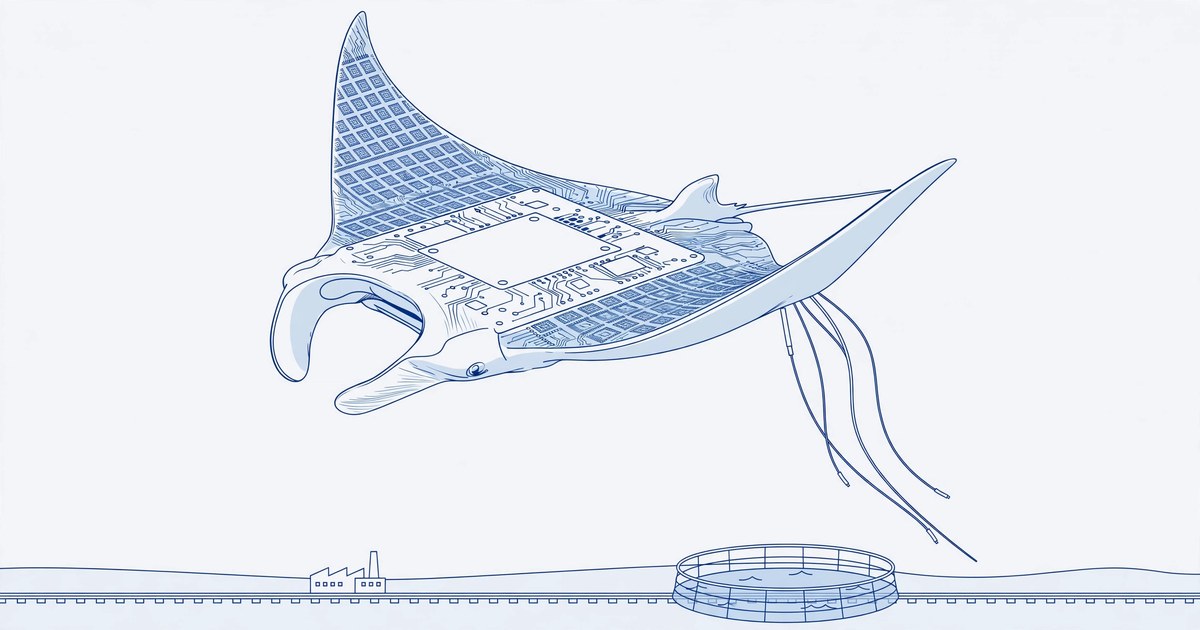
Tokyo Artisan Intelligence (TAI): a Tohoku University spinout in Yokohama's Kohoku Ward that builds edge AI for railways, factories and fish farms — and now designs its own chip. Its edge AI is also used at aquaculture sites.
¥1.27 billion
Series C first close
Announced October 26, 2026; the split between equity and debt is undisclosed
40nm
A mature node, chosen on purpose
Fabricated by UMC at 40nm under the company's plan; the test chip Sting Ray used the same process
Q4 2027
Fabrication of the mass-production version
Read the roadmap by its verbs: this quarter makes the chip, it does not ship it — evaluation boards follow in Q1 2028
Revenue and orders are undisclosed, and no reproducible performance benchmark has been published. Every judgment here is staked only on the public timetable and peer precedent.
Pages · 2/7
One shareholder list, half a customer list
Meet the protagonist first. TAI runs three businesses: edge AI solutions (today's revenue), the software and on-premise servers that go with them, and its own chip, Manta Ray (this article's bet). The problems it says it is solving, in the company's own blunt words: sites have no people — and general-purpose chips draw too much power to fit inside a sealed box on site.
A five-way split of labour
TAI
Supplies the AI technology and product definition
Kohoku Ward, Yokohama; a Tohoku University spinout with 35–60 people depending on who is counted; its own SEASIDE platform is the chip's first buyer
Oppstar
Draws the chip in Malaysia
A Penang IC design-services firm responsible for Manta Ray's full design and physical implementation; signed a strategic cooperation framework with TAI in June 2026. Its Japanese arm, Oppstar Japan, collaborated on the test chip
UMC
Makes the chip in Taiwan
Fabrication on a 40nm process under the company's plan; neither design implementation nor manufacturing happens inside Japan
Shareholder-customers
Supply money, and buy product
JR Kyushu, Tokyo Keiki and Watakyu — all three collaborated first and invested later; the shareholder list and the customer list largely overlap
ADT
Sells the chip to strangers
A Tokyo sales partner that signed in September 2026 and co-develops the evaluation board with TAI; chip sales targeted to begin by the end of November 2027, with a distributor network to follow — a channel still under construction
Remember this web: before the chip exists, the "insider" demand is already lined up. What needs verifying is whether anyone outside the web will buy.
Pages · 3/7
The "build it" wall is about $0.3–1.5M. The "sell it" wall has no price tag
About $0.3–1.5M
The road it took: estimated cost of a 40nm full mask set
An industry-guide estimate, not TAI's actual spend (undisclosed)
About $40–50M
The road it didn't take: design cost one generation ahead, at 28nm
Tokyo Electron (TEL) public materials; roughly 30× the mask-set figure — a different cost type (design cost vs mask-set estimate), compared for order of magnitude only
The first wall is low because the company chose a mature process. The second wall is time: the design tool customers need for adoption reaches alpha only in Q1 2027, the first evaluation board an outside customer can hold arrives in Q3 2027, and the channel that sells to strangers targets its first sales for the end of November 2027. Money can pay for a tape-out; it cannot buy a customer's adoption cycle.
Pages · 4/7
A timetable you can tick off, box by box
July 2026 · Test chip evaluation completed
Sting Ray was designed, fabricated and evaluated on UMC 40nm — the one box already ticked
Q1 2027 · Design tool, alpha release
The customer's clock starts here; without tools, no chip can be adopted
Q2 2027 · Engineering-sample chip fabricated
Mind the verb: fabricated — not yet in any customer's hands
Q3 2027 · Engineering-sample evaluation board provided
The first board an outside customer can hold; ADT's joint sales structure completes in the same quarter
Q4 2027 · Mass-production-version chip fabricated
The box most easily misread in the whole table — made, not shipped in volume
Q1 2028 · Mass-production evaluation board provided
Customer verification of the production version starts only here
The roadmap's source is TAI's own two official releases (July 6 and October 21, 2026 — the wording agrees). From here on, every milestone is a checkpoint for revisiting this article.
Pages · 5/7
This field just buried two players far richer than TAI
About ¥5 billion → dissolved
LeapMind's total funding and its end
A Japanese edge-AI peer, dissolved in July 2024; its CEO said it had "failed to prove its value"
$340 million → acquired cheaply
Hailo's total funding and its end
Peak valuation $1.2 billion; acquired by Microchip in July 2026 at an undisclosed price
Over $110 million → shipping in volume
EdgeCortix's total funding and its present
The field's front-runner; TAI's publicly traceable funding totals about ¥2.76 billion
Three different endings — but not one of them died because the chip could not be built.
Pages · 6/7
The chip's first buyer is the company itself
3
Real buyers sitting on the shareholder list
JR Kyushu, Tokyo Keiki and Watakyu — each collaborated first, invested later
JIS E4031
The railway-vehicle standard the SEASIDE platform has already passed
The next-generation SEASIDE will carry Manta Ray — the production version's first demand is internal
LeapMind held only technology licences and had no demand of its own. TAI's chip has not shipped, yet its first installation slots are already written into its own platform and its shareholder-customers' sites. That is a structural difference, not a technical one.
Pages · 7/7
Four signals to watch
Proven so far — the test chip finished evaluation on the same process, scoped to hardware implementation and basic functions (configuration, clock and I/O control); every shareholder-customer stayed in through the Series C; the design split and the METI grant are signed and in place. Not yet proven — production yield (never disclosed, and not estimated here), a performance benchmark meeting the reproducibility standard (none found in this review), externally verifiable orders, chip-business revenue.
Do the 2027 samples and boards land on schedule?
Engineering-sample chip fabricated in Q2, evaluation board provided in Q3 — the first checkable signal
Does reproducible performance data appear?
Data that names its model, precision and test conditions — not a marketing peak
Is there a named outside customer verification or order?
A name beyond shareholders and its own platform is what counts
Do the tools and long-term supply take shape?
A production design tool; ADT's distribution and long-term supply structure
That the chip can be built, this magazine believes. Whether it can be sold — the orders will say.
Tohoku spinout TAI skips the leading edge on purpose: for railways and factories it chose UMC 40nm and a reconfigurable architecture — cheaper tape-out, stable supply; a mature node is not inherently lower-power. Production chips are fabricated in Q4 2027; the test: a paying outsider by end-2028.
Key takeaways
- Manta Ray is a reconfigurable AI semiconductor (an FPGA's rewritability with an ASIC's efficiency), planned on UMC's 40nm process — a deliberate refusal to chase the leading edge: what it buys is a tape-out cost an order of magnitude lower (a 40nm full mask set estimated at about $0.3–1.5M, against a 28nm design cost of $40–50M, TEL public materials; industry estimates, not TAI's actual spend), the supply stability of a mature process, and performance enough for the field. A mature node is not inherently lower-power or more reliable, though; suitability can only be proven by a specific product's measurements. Its power target is a whole-system figure — 10W or less for the system as a whole (chip plus control CPU and the rest, cooled by heatsink alone), not a single-chip number (a company target, not a measurement). The test chip Sting Ray completed evaluation in July 2026, on the same 40nm process (verification scoped to hardware implementation and basic functions).
- On October 26, 2026, TAI (Tokyo Artisan Intelligence) announced the first close of its Series C: ¥1.27 billion in total, a third-party allotment led by Mitsui Sumitomo Insurance Capital (with Watakyu HD, Tokyo Keiki and ADT among the allottees) plus a loan from Mizuho Bank; the equity/debt split is undisclosed. Publicly traceable funding to date totals about ¥2.76 billion. A funding total is not a valuation, not revenue, and not a customer contract.
- The official roadmap's five cells (itemised on Deck page 4): design-tool alpha in Q1 2027; engineering-sample chip fabricated in Q2; engineering-sample evaluation board in Q3; mass-production-version chip fabricated in Q4; mass-production evaluation board in Q1 2028. Q4 is fabrication, not volume shipment.
- The absence of a qualifying benchmark is itself a finding: this review found no published benchmark — no TOPS, TOPS/W or latency figure — that names its test model, arithmetic precision, batch size and power boundary and that a third party could reproduce. On the public evidence, Manta Ray's performance is still a hypothesis.
- Peer precedent: LeapMind raised about ¥5 billion and dissolved in 2024; Hailo raised $340 million and was acquired by Microchip in 2026 at an undisclosed price; EdgeCortix has raised over $110 million, is shipping in volume, and holds a validation memorandum from the US Defense Innovation Unit. None of the three died because a chip could not be built.
- Our judgment, in two questions: the technical question — the architecture has a mechanism-level value for specific industrial workloads, unproven by public data; the commercial question — the life-or-death line is whether a paying adoption beyond its own platform and shareholder-customers appears by the end of 2028 (this magazine's own observation deadline, not a company plan). The falsifiers are in Sections 1 and 11.
Start with its most consequential choice: it deliberately does not chase the leading edge — for sites like these, it chose a mature 40nm process and a reconfigurable architecture. That choice, a test chip already run on the same process, and a professional design team behind it mean TAI will most likely fabricate its mass-production-version chip on its own timetable — the risk of "building it" sits at the lowest level in this field. But the mass-production evaluation board reaches customers only in the first quarter of 2028, and the real life-or-death line sits after that.
By the end of 2028 (this magazine's own observation deadline), it must land a paying adoption beyond its own platform and its shareholder-customers; failing that, this company will have won the chip and lost the business. Only two things would overturn this judgment: fabrication of the mass-production-version chip still unfinished past the end of Q1 2028, or a paying adoption by a non-shareholder appearing before the deadline — if either happens, this magazine will publish a correction.
The company card: Tokyo Artisan Intelligence (TAI)
Tokyo Artisan Intelligence Co., Ltd. was founded in March 2020 and is headquartered in Shin-Yokohama, Kohoku Ward, Yokohama — a spinout of Tohoku University. Founder Keiki Nakahara is a Tohoku University professor serving as CEO and CTO; since 2025 he has shared the representative role with COO Kazumasa Okayasu. The registered business description is short: research, development and sale of AI semiconductors and edge AI solutions. What that expands into is the next two cards.
Three businesses
One: edge AI solutions — the current revenue engine. The lead product, SEASIDE, is an edge AI module designed for each use and built to be embedded in equipment (an FPGA at its base), and it has passed the tests of the railway-vehicle standard JIS E4031. The solutions have moved into demonstration and adoption at railway, municipal, aquaculture and infrastructure-inspection sites (company claims; deployment volumes and contract values have never been disclosed — the specific deployment record is in Section 3). Two: software and on-premise AI products. ITAMAE: edge AI software technology that organises and optimises the data a site collects, tuned to each use. HARBOR: an AI server that sits at the customer's site, manages data and AI models and retrains them in place — no cloud required. SASHIMI: an AI computing unit for the infrastructure industry that packages SEASIDE, HARBOR and ITAMAE together. NIGIWAI: people-flow analytics software commercially launched in June 2026; the video is processed on the camera itself and never sent out, counting footfall and dwell time for municipalities and commercial facilities. Three: its own chip — this article's protagonist. The reconfigurable chip Manta Ray, the new bet that grew out of the solutions business; the next-generation SEASIDE will carry it.
What it is trying to solve
In its Series C release, the company names two problems (the company's own framing). The first is AI's power consumption — as AI spreads, the electricity drawn by data centres and devices keeps climbing, and demand for low-power AI chips is surging. The second is the missing workforce on site — as the working population shrinks, labour shortages across manufacturing, logistics and infrastructure grow more severe, and the need for "physical AI" that can work on site rises with them. The infrastructure layer has hard numbers under it: of roughly 730,000 road bridges nationwide, the share standing for more than 50 years will rise from about 39% to about 63% by 2033 (Ministry of Land, Infrastructure, Transport and Tourism), while the people who inspect them bridge by bridge only grow fewer. TAI's answer is to make AI small and frugal enough to sit inside a sealed box beside a track, on a train or in a factory, and judge on the spot — waiting for neither the cloud nor a person. Manta Ray's job in this picture is to push the unit cost of that answer down one more step: general-purpose chips cannot pass the site gates of power, heat and enclosure size, and only a chip of its own gives on-site AI a chance to move from one pilot at a time to deployment at scale. All of the above is the company's statement of purpose, not this magazine's conclusion; whether it can be delivered is what the sections below test.
TAI and Nakahara: the side that supplies technology and definition
In this split of labour, TAI keeps its own hands on exactly three things: the AI technology itself, this chip's product definition, and the solutions layer closest to the customer — every other step is handed out. It is both the chip's designer and its first customer: fitting Manta Ray into the next-generation SEASIDE is a published plan. Headcount is 35–60, depending on whether contractors and partner staff are counted.
Oppstar and UMC: one draws, one makes
The chip's full design and physical implementation — turning logic into the actual circuit patterns on a wafer — is carried, under the strategic cooperation framework, by Oppstar, an IC design-services company in Penang, Malaysia. The two companies signed a statement of work in spring 2026 and a strategic cooperation framework in Kuala Lumpur in June. One step earlier, the test chip Sting Ray's design collaboration came from Oppstar's Japanese arm, Oppstar Japan, in the same city of Yokohama — collaboration at test-chip level has already happened; collaboration at production-version level is signed, not yet delivered. Manufacturing, under the company's plan, goes to Taiwan's UMC on a 40nm process. In other words, neither the design implementation nor the manufacturing of this "Japanese AI chip" takes place inside Japan — but technical control is not judged by which country hosts the factory: the architecture and AI hardware technology, the design tools and the product definition are all in TAI's hands, and those are its real assets (Section 2, final part).
ADT: the side that sells to strangers
Tokyo-based ADT is TAI's market-development partner: the two signed in September 2026, and co-development of the evaluation board began the same month. Together they are building the sales and technical-support structure, aiming to begin chip sales within 2027 — with sales at the end of November 2027 as one milestone for the distributor network — and the evaluation board's manufacturing and long-term supply structure are also within their discussions. ADT also appears on the Series C investor list — shareholder first, seller second. But the line must be drawn: a signed agreement and started co-development are not a finished channel. Until the distributor structure exists, external sales of the chip have not really begun.
The shareholder-customers: they fund it, and they buy it
JR Kyushu and JR East Consultants joined in the 2025 Series B. Tokyo Keiki co-developed a railway track-inspection AI system with TAI and invested in October 2026. Watakyu invested after running TAI's automation pilot in its own linen factories. What the three share: each used the product at its own sites first, then paid to become a shareholder. This list is TAI's largest structural difference from a pure chip company.
METI: standing on the Malaysia line
In September 2026, the Ministry of Economy, Trade and Industry's Global South co-creation grant (large-scale ASEAN demonstration) adopted TAI's Japan–Malaysia edge-AI chip industry demonstration project; the grant amount is undisclosed. The money's significance is not its size — it is the official stamp it puts on a division of labour that designs in Malaysia and manufactures in Taiwan.
1. The thesis
First, separate fact from judgment.
The facts: on October 26, 2026, an unlisted company in Yokohama announced a ¥1.27 billion first close of its Series C. Its test chip had completed evaluation three months earlier, and its production version's timetable runs to the first quarter of 2028. The company is Tokyo Artisan Intelligence (TAI). What it makes is AI that runs inside small boxes at railway sites, factories and fish farms — "edge AI" in the industry's term: the computation does not travel back to the cloud; it finishes where the data is born. Its most unusual choice is the process: while the whole industry chases ever more advanced nodes, it deliberately chose the mature 40nm node — and designed its own reconfigurable chip for it. Why is the first question this article answers.
Our judgment must be split into two questions, because their states of evidence are entirely different:
The technical question: does TAI's architecture hold clear value under specific industrial workloads? Our answer: the mechanism is coherent; the data does not prove it. The field it has chosen is real, and every design choice has a reason rooted in the field. The test chip verified hardware implementation and basic functions, but this review found not one published set of performance numbers — conditions named — that a third party could reproduce. Whether the value exists is, on the public evidence, still a hypothesis.
The commercial question: is that value enough to make customers abandon mature platforms and bear a new chip's adoption, maintenance and long-term supply risks? Our answer: this is the company's real life-or-death line, and its own roadmap pushes it into 2028 — the mass-production evaluation board reaches customers only in the first quarter of 2028, and within the first customer-verification cycle after that (this magazine sets the boundary at the end of 2028), it must land a paying adoption beyond its own platform and its shareholder-customers.
Together, the thesis: if this company loses its bet, it will lose after the chip, not on it — and "after the chip" starts a year later than most coverage suggests. A mature process, an architecture already verified in silicon, and a professional design team have pushed the risk of "building it" to the lowest tier in this field. What happens if the judgment is wrong is written in Section 11: if either of two falsifiers triggers, this magazine will publish a correction.
2. Meet the cast: a five-way split, and how the money flows
From drawing to customer, this chip passes through five roles and three countries. The deck's second page listed the names; here is how the money moves.
Investor and bank money enters TAI first. Of the ¥1.27 billion Series C first close, the equity part comes from a third-party allotment led by Mitsui Sumitomo Insurance Capital (Watakyu HD, Tokyo Keiki and Tokyo Keiki Rail Techno, ADT), and the debt part is a loan from Mizuho Bank; the company has not disclosed the ratio between them. METI's grant stands alongside, aimed at the Japan–Malaysia industry demonstration; its amount is undisclosed.
Money flows out of TAI in three directions. First, design fees to Oppstar in Penang, Malaysia, which under the framework carries Manta Ray's full design, physical implementation and verification. Second, tape-out and fabrication fees, under the plan to UMC in Taiwan. Third, its own solutions business — still its real revenue engine today. Once the chip exists, it flows back not to the open market but to the company's own SEASIDE platform and the sites of its three shareholder-customers. The road to strangers opens only when ADT's distributor structure is built.
Two judgments about this structure must be set down first. First, a division of labour is not hollowness. Technical control over a chip is judged by who holds the architecture and design IP, who holds the design tools that turn a model into a chip configuration, and who holds system integration and product definition — all three sit with TAI. A factory in Taiwan and design services in Malaysia are the normal shape of the fabless model, not evidence of an empty core. Second, a signed agreement is not a finished system. Oppstar's framework, UMC's process plan, ADT's channel targets and METI's grant adoption are all signed paper; between that paper and production delivery stand three gates not yet passed — engineering samples, evaluation boards, customer verification (Section 8 sets them side by side). Set these two down, and the analysis that follows will not slide into either "a Japanese chip that depends on foreigners" or "big-name partnerships equal success".
3. Where this company came from
TAI's starting point had nothing to do with chips: in 2020 it began with the digitalisation of aquaculture, and the same year took over the AI business of Sinkom Co., Ltd. The "tai" (sea bream) pun inside Tokyo Artisan Intelligence comes from the fish farms — and afterwards the whole product line took seafood names: SEASIDE, ITAMAE (the sushi chef), HARBOR, SASHIMI, NIGIWAI; the chips are Sting Ray and Manta Ray.
The technology comes from two things in Keiki Nakahara's laboratory at Tohoku University: neural-network compression — pruning and slimming a trained model until it can run on a small chip — and the implementation craft of landing a compressed network efficiently onto hardware. The solutions business was the first job for both: JR Kyushu track monitoring, obstacle detection on Shinkansen confirmation cars, municipal projects, aquaculture and infrastructure inspection — all, by the company's account, in demonstration or adoption (deployment volumes and contract values have never been disclosed; this magazine records them as company claims).
The lead module on the company card, SEASIDE, is now about to have its heart replaced — that is the question of the sections that follow. The step just before it came in October 2025, when TAI and Tohoku University set up the Reconfigurable AI-Chip Co-Creation Institute — a clear signal of the turn from "a solutions company that uses FPGAs" to "a fabless company that designs its own chips". In August 2026, at its own event, the company demonstrated the test chip live and published the full roadmap for Manta Ray. The second generation, "Whale Shark", is targeted around 2030 and may stack memory and analogue circuitry — that is the next betting table; this article does not bet on it.
4. The compute the field needs is not the compute the data centre sells
Before comparing any chips, walk through what a site actually computes. A detection box beside a track, from seeing to acting, passes through five steps:
Sensing
Cameras and sensors turn the site into data — the speed of this step is set by the sensors, not by the AI chip
Preprocessing
Resizing, correction, denoising — shaping data into a form the model can read, usually on a general-purpose processor
AI inference
The neural network delivers a judgment: is something wrong, and what is it — the step chip vendors advertise loudest
Decision
Inference results are combined with thresholds, rules and safety logic into a single decision
Control
Alarm, slow down, stop — the decision lands in the physical world, where lateness is an accident risk
Keiki Nakahara made this point bluntly at the company's August 2026 event (Mynavi reporting): what industrial sites care about is not how fast AI inference itself runs, but the total system latency — preprocessing, data movement to and from a GPU, and actuator control included. Accelerate inference on a GPU all you like; if preprocessing still crawls on an Arm processor and data still ferries between chips, the chain's latency does not fall. For railways and robots, the lag between a recognition result and an action is itself a risk.
That is the shape of edge AI demand, and it is nearly the opposite of data-centre demand:
- Latency belongs to the whole system, not to one chip's benchmark. If any of the five steps is slow, the site experiences slowness.
- The network cannot be assumed. Beside tracks, in tunnels, at fish farms, connections are closed, intermittent or simply absent — the judgment must close locally. The cloud's cleverness cannot enter such sites.
- Power and heat are hard constraints. Sealed enclosures, no room for fans, a train's power supply — budgets are counted in watts. Heat is not an efficiency question; it is a whether-it-fits question.
- Equipment lives are counted in decades. Railway and infrastructure equipment runs for ten years and more once installed, while algorithms must be updated yearly: hardware cannot be frozen for a decade, and supply cannot be cut in three years.
- The load is still growing. Multiple cameras, several models running at once, local large language models — the company states Sting Ray's assigned problem precisely: "the growth of power consumption from running multiple AIs simultaneously" (TAI official release).
With the demand in focus, TAI's choices gain coordinates: what it needs is not stronger compute, but compute that, within a watt budget, an enclosure and a disconnected network, can run all five steps — and still change its task. That demand is real. The next question is how far today's products stand from it.
5. First, the alternatives: how strong the incumbents are
The fact most unfavourable to TAI — and therefore the one to state first — is that customers can choose today, and everything they can choose has specifications, prices and an order button.
NVIDIA's Jetson is the default option. On NVIDIA's official product page, the Jetson Orin Nano is rated at up to 67 TOPS at 7–15W, starting at $199, with the Orin NX, AGX Orin and the new Thor above it. What makes it hard to beat is not the numbers but the JetPack software ecosystem — CUDA, TensorRT, the Isaac robotics frameworks, more than a decade of accumulated developers — and module availability windows that officially run, typically, five to ten years. (All figures are vendor-stated; TOPS precision and test conditions differ by model, and this article does not build a performance ranking from them.) For a customer, Jetson means: order today, documentation complete, and whatever problem you hit, someone in the world has hit it before you.
Hailo represents the dedicated-accelerator route. Its Hailo-8 is rated at 26 TOPS (vendor-stated) and ships in M.2 and mini-PCIe forms that plug into an existing industrial PC; it has been shipping for years. Its position: change no host, change no architecture, add one AI acceleration card.
AMD's adaptive platforms (formerly Xilinx) are the closest of all — close enough to be inside TAI's own product. On TAI's own demonstration materials, the platform advances by generation: SEASIDE-R6 runs AMD's Kria system-on-module, the current production generation R7 runs Efinix's Titanium FPGA (per Mynavi's reporting), and only the planned next generation switches to Manta Ray. Which is to say: the first opponent Manta Ray must displace is not a stranger — it is the solution TAI ships today: programmable, mature in tooling, already in customers' hands. The strategic meaning of this product line deserves to be marked separately (this is this magazine's research hypothesis, not an accomplished fact): TAI's route is to run the platform, the customers and the field data first on bought reconfigurable hardware, then migrate the main compute, step by step, to its own silicon — bought hardware as the stepping stone to in-house silicon. Mind the limits of "step by step": the next-generation SEASIDE is still a Manta Ray plus a companion FPGA on interface duty; in-house silicon takes over only the AI compute. Whether the route ultimately holds will be tested not by narrative but by four things: whole-system deployment cost, reproducible measured performance, the maturity of the software tools, and the reliability of long-term supply. Manta Ray must first beat Kria and Efinix inside its own product before it can talk about beating anyone else.
EdgeCortix is the domestic front-runner in the same field: also in Japan, also building edge AI chips, with SAKURA-II already shipping in volume — and, in June 2026, a success memorandum from the US Defense Innovation Unit on its platform readiness, the record of an institutional customer verifying it through its own process. Its existence proves the road can be walked, and it measures TAI's distance from "verified".
Across the seven dimensions — performance and energy efficiency; programmability and model support; development tools and ecosystem; industrial deployment and long-term supply; product maturity; price and total cost of ownership; customer switching costs — the incumbents share one portrait: no cell is empty. Jetson is strong on ecosystem and maturity, Hailo on plug-in ease, the FPGA platforms on programmability and interface flexibility, EdgeCortix on already shipping. TAI, on every dimension, is still in the future tense.
So this article's hardest counter-question must be answered head-on: if a Jetson, a Hailo or a Kria is already enough, why would a customer bear the adoption, maintenance and long-term supply risks of a new chip whose mass-production evaluation board arrives only in 2028?
TAI's possible differentiation comes down to four cards, and every one of them is still unproven. First, system-level optimisation — a company that builds both the chip and the solutions can feed field data and application knowledge directly into the chip's definition, a loop no pure chip vendor has. Second, power under parallel AI workloads — the reconfigurable architecture's efficiency on concurrent loads is the problem the company publicly names, but it has published no numbers for it. Third, total cost — if a 40nm chip is cheap enough, whole-unit prices have room to fall, but no unit price has ever been published. Fourth, domestic support and long-term supply — if ADT's sales, support and long-term supply structure gets built, it is a real decision factor for Japanese industrial customers; it is still under construction.
The conclusion belongs here, not at the end: today, TAI cannot answer that question with public evidence. Over the next two years it must turn those four cards, one by one, into checkable facts — or customers have no reason to leave the incumbents. That is not pessimism. It is the true meaning of the next milestone on its own roadmap.
6. Why 40nm? TAI's answer is a reconfigurable architecture
First, what "reconfigurable" means — do not read it as "a chip that can become any chip it wishes".
Lay out the four kinds of computing device. A CPU is a general-purpose processor: it computes anything, optimised for nothing in AI. A GPU computes matrices with massive parallelism — strong on throughput, at the price of power and data movement. An FPGA has circuit logic that can be rewritten after shipment — flexible, but the programmable fabric held in reserve for generality draws power and area around the clock. An ASIC/NPU freezes its circuits at tape-out for specific operations — the most power-efficient, but a changed task means a new chip. TAI's reconfigurable architecture walks the narrow road between FPGA and ASIC: inside the chip sits an array of processing elements specialised for neural-network multiply-accumulate operations, and the routing channels between elements, together with the mapping of computation onto them, can be rewritten after shipment. In Sting Ray's official technical description, optimisation of the routing channels is named the core of the architecture — a simple structure whose wiring state can be observed and controlled directly. The flexibility comes from rewritable mappings and routing; the efficiency comes from elements born only for AI arithmetic. The official summary is "the reconfigurability of an FPGA combined with ASIC-like efficiency" (the company's description).
The route carries real constraints, and they must be written alongside: the models and operators it supports have boundaries — not every network maps efficiently; what can be reconfigured is routing and mapping, not a metamorphosis into another chip, and reconfiguration itself costs time and tooling; the dependence on design software and compilers is extreme — if the tools fail, the flexibility exists only on paper; a neural network's bottleneck is often memory and data movement rather than arithmetic, and elements packed ever denser still idle if they cannot be fed; and for customers, a development discipline unlike either GPU or FPGA carries a real learning cost. Among these constraints, the tools become a hard milestone on the calendar in Section 8.
One more layer of the split: Manta Ray computes; it does not do I/O. In the evaluation-board form the company has published, Manta Ray specialises in AI computation, while the wildly varied inputs and outputs — cameras, sensors, vehicle buses — are carried by a companion FPGA. The logic: interfaces differ at every site, computation is comparatively uniform. Leave the changeable part on the rewritable FPGA, and the AI die itself can stay small and simple, with the same chip serving different sites. The cost is equally real: what a customer buys is never one chip, but a set — chip plus FPGA plus tools — and cost and complexity must be counted for the set.
The process: UMC 40nm. Under the company's plan, both Sting Ray and Manta Ray use UMC's 40nm — a mature process chosen deliberately. Its possible advantages first, each with its condition: design and tape-out costs an order of magnitude lower (numbers in Section 8), a matter of survival for a company whose traceable funding is under ¥3 billion; ample, stable mature-node capacity, with no need to fight the world's giants for fab lines; and for industrial loads with watt budgets and decade lifetimes, its speed and density suffice, with generous design margins. Then its limits, stated just as plainly: a mature process is not inherently lower-power — transistors grow more frugal with each generation as a matter of physics, and the same work on an advanced process often completes at lower voltage; 40nm's compute density per unit area is low, so the die grows or performance caps; and its cost advantage holds only when shipment volumes match the product definition — at small volumes, mask and development costs refuse to amortise just the same. So this magazine's formulation is: 40nm is an account TAI has calculated among cost, supply and target load — not a law that "40 suits industry better than 3". A node number by itself proves no suitability; only a specific product's measurements can.
The three routes' accounts, side by side (sources and calibres in the note):
| Cost of changing the task | Power | Unit cost | Adoption threshold | |
|---|---|---|---|---|
| FPGA | Rewrite the configuration — the lowest of the three | General-purpose fabric always on; first to hit a sealed box's power ceiling (qualitative) | Highest chip unit price (qualitative) | Toolchain is mature; adoption can start today |
| Fixed-function ASIC | Circuits are frozen at tape-out; changing the task means building a new chip | The lowest of the three (qualitative) | Lowest at high volumes; at low volumes, eaten by mask costs | The task must be frozen first, and the chip must be waited for |
| Reconfigurable (the Manta Ray route) | The mapping can be rewritten after shipment — between the two | System target of 10W or less (company target) | 40nm mature process; mask set about $0.3–1.5M (industry estimate) | The design tool reaches alpha only in Q1 2027 — until then, customers cannot begin adopting |
Note: except where figures are marked, this table is a qualitative, architecture-level comparison and does not correspond to measurements of any specific product; the TAI figure in the power column is a company target, not a measurement, and it is a whole-system figure (chip plus control CPU and the rest), not the power of a single chip.
7. What Sting Ray proved — and what Manta Ray has not yet proved
This section does one job: pin "verification that has happened" and "verification that has not" to separate parts of the wall.
What Sting Ray proved, per TAI's own official release, comes to four items. First, architectural exploration: on UMC 40nm, it explored and optimised a structure whose processing circuits can be changed to fit the use and the AI model — reconfigurability moved from paper onto silicon. Second, the routing channels: the architecture's core wiring was built in a form whose state can be observed and controlled directly, with verification tooling in place. Third, design and verification software: the design software that lands a user's circuits on this chip, and the verification software that confirms a fabricated chip works, were developed by TAI itself — the toolchain's first brick was laid by its own hand. Fourth, process: the full run from design and fabrication to functional confirmation on an evaluation board and the establishment of control software was carried through under TAI's lead with Oppstar Japan's collaboration; Keiki Nakahara says the test chip worked on its very first tape-out (a statement at a company event, carried by media reporting).
The August 2026 live demonstration must also be weighed. Per Mynavi's on-site reporting, the demonstration consisted of LED blinking and square-wave audio output — it verified that configuration writes, clock control and external I/O control on the chip genuinely work. That is a solid step: it showed the design tool can deliver a configuration into the chip and the chip acts on it. But it demonstrated no neural-network workload result of any kind — no image-recognition frame rate, no measured power draw, no same-conditions comparison against any incumbent product.
From this follows one of this article's independent research findings, owed to no standpoint: this review found no published benchmark for Manta Ray (or Sting Ray) that meets the standard. The standard is specific: a TOPS, TOPS/W, latency or throughput figure that names its test model, arithmetic precision (INT8, INT4 or FP16), batch size, power boundary and software version. Searched against that standard, TAI's official releases and the public reporting come back empty. Even the most-quoted power number must be read with the right boundary: 10W is not the power draw of a single Manta Ray chip. In a November 2025 interview, Nakahara described a target for the whole system — the chip still needs a control CPU beside it; the system total is to be held to 10W or less, cooled by a heatsink alone, at roughly a fifth to a third of the conventional system's power (Mynavi's reporting). Nikkan Kogyo Shimbun compressed this into a chip power of about 10W, half the existing solution. The two accounts do not match; this magazine follows the CEO's own system-level wording — and on either account, the figure is a target, not a measurement. The absence of a qualifying benchmark is itself an important research conclusion: it means that of the four differentiation cards in Section 5, not one can today be cashed in as evidence; and it means that any claim, from anyone, that "Manta Ray outperforms product X" has no public basis. This magazine does not manufacture such rankings.
What Manta Ray still has to prove, item by item: yield at production scale (undisclosed, and not estimable); the actual prices of the chip and the evaluation board (unpublished); reproducible performance and power data (none meeting the standard was found in this review); the design tool's maturity, from alpha to a state where a customer can complete adoption unaided (the milestone has not arrived); and any installation, order or purchase commitment beyond shareholders and its own platform (as of today: none visible in public sources — the solutions business's deployment record belongs to the solutions business and cannot be booked to the chip's account; this article does not cross that line anywhere).
8. Two walls, and one roadmap
Chip startups' deaths are usually filed under one phrase, "failed at mass production". Taken apart, there stand two entirely different walls: the first is called "building it", the second "selling it". The two walls in front of TAI stand at very different heights.
The first wall: "build it", about ¥100–200 million high.
The hardest single cost in turning a chip from drawing into object is the mask set — the templates that print circuit patterns onto wafers; making a full set is the main cost of a tape-out. Its price climbs steeply with the process node. Tokyo Electron's (TEL) public materials price the road not taken: one generation ahead at 28nm, the design cost alone runs $40–50M, with mask sets accounting for several million dollars of that; on the road taken, a 40nm full mask set, by industry-guide estimates, runs about $0.3–1.5M. In other words, by choosing 40nm, TAI pressed the height of the "build it" wall down to roughly the ¥100–200 million scale (industry estimates, not TAI's actual spend — its actual tape-out expenditure has never been disclosed). The ¥1.27 billion it raised pays that bill with room to spare, including a reserve for a respin: if the production version needs a fix, one respin means paying for another mask set and waiting months — the main residual risk on this first wall.
The second wall: "sell it" has no price tag — only a calendar.
Lay the official roadmap out box by box (the wording of TAI's releases of July 6 and October 21, 2026): Q1 2027, the design tool's alpha release. Q2, the engineering-sample chip is "fabricated". Q3, the engineering-sample evaluation board is "productised and provided", with ADT's joint sales structure completed in the same period. Q4, the mass-production-version chip is "fabricated". Q1 2028, the mass-production evaluation board is "provided". Mind the verb in every box: within 2027, all a customer can actually hold is an engineering-sample-grade evaluation board; the production version is merely fabricated in Q4 2027, and its evaluation board waits one more quarter. Reading Q4 as "volume shipment" is this table's easiest and most consequential misreading — earlier versions of this article were loose at exactly this point; this version corrects to the official wording.
Then comes the industrial customer's adoption cycle. For a railway or factory customer to design a new chip into its equipment means design-in, standards review and safety review, on a cycle counted in years — TAI's own SEASIDE passing JIS E4031 is both precedent and reminder. Then there is production working capital: wafers are paid for up front and inventory accumulates before any customer money arrives; a chip business sinks substantial cash before it earns. And finally channel and supply: ADT's targets are to begin chip sales within 2027, with sales at the end of November as a milestone for the distributor structure, while the evaluation board's manufacturing and the long-term supply structure are still being built in its discussions with TAI — channel, evaluation-board production and long-term supply all read "under construction".
Mark the supply chain's maturity on four levels — agreements signed, technical verification, product fabrication, customer delivery — and TAI's position today is: agreements complete (framework, grant and channel contracts all signed); technical verification finished at test-chip level; product fabrication scheduled in 2027; customer delivery of the production version scheduled in 2028. Not a shameful position — but two levels short of "the system is built".
Stack the two walls and the conclusion is clear: ¥1.27 billion is enough to clear the first wall, respin included. The second wall is not a money problem — tools, samples, evaluation boards, certification and channel each keep their own calendar, and every one of those calendars points at 2027–2028. That is why this magazine draws the life-or-death line at the end of 2028: the mass-production evaluation board reaches customers in Q1, and the time left for the first full round of customer verification is that one year.
9. The peers' ledger
To judge a chip startup, first look at the field's base rate. The three peers with the most reference value each prove one thing — and each fails to prove one thing:
| Company | Model | Money raised | Now | What it proves |
|---|---|---|---|---|
| LeapMind (Japan) | AI-inference IP licensing | About ¥5 billion in total | Dissolved in July 2024 | Technology adopted by majors is not the same as a viable business |
| Hailo (Israel) | Standalone chip sales | $340 million in total; peak valuation $1.2 billion | Acquired by Microchip in July 2026; price undisclosed (reported far below peak) | Building the chip, and selling it, still may not sustain a standalone company's valuation |
| EdgeCortix (Japan) | Chip plus software platform | Over $110 million in total | SAKURA-II shipping in volume; a 2026 success memorandum from the US Defense Innovation Unit | Someone has walked this road through to production and institutional validation — and it marks TAI's size gap |
LeapMind is the case that stings Japanese industry most: its low-power AI-inference IP was adopted by major companies and well regarded; it announced its own chip at the end of 2023 and dissolved roughly nine months later, in July 2024. What it proves: between praised technology and a viable business lies an entire set of demand and cash flow. It does not prove TAI must fail — LeapMind held only IP licences, with no customers or field sites of its own; TAI's structure is precisely the reverse.
Hailo proves a further layer. It did everything right — the chip reached production, the customers were real, the valuation once touched $1.2 billion — and still ended up acquired by Microchip at an undisclosed price. It does not prove the field lacks demand (its shipments were real). It proves the difficulty of scaling revenue as a standalone edge-chip company: fragmented customers, price pressure, and a channel-and-toolchain war to refight every generation. Fairness also records this: Hailo still ships today and its product line still updates — acquisition was the ending of its standalone company, not the failure of its technology.
EdgeCortix is the measuring stick: also in Japan, also in edge AI chips, with over $110 million raised (roughly six times TAI's publicly traceable total — currencies and calibres differ, so treat it as a scale reference only), and SAKURA-II already shipping in volume, with a defence customer's process validation behind it. It proves that "a Japanese company builds an edge AI chip and reaches production" is itself achievable. It also recalls that the player who reached that step held several times TAI's money — and a verification record TAI does not yet have.
10. Where the money comes from, what it must feed — and what each side wants
First, the nature of the funding event itself, because it is the easiest thing in this article to misread: ¥1.27 billion is an amount raised — not a valuation, not revenue, and not a customer contract. It consists of two entirely different kinds of money: the equity part is a third-party allotment led by Mitsui Sumitomo Insurance Capital (allottees: Watakyu HD, Tokyo Keiki and Tokyo Keiki Rail Techno, ADT); the debt part is a loan from Mizuho Bank. The company has not disclosed the ratio between them, and this magazine does not divide it. Money arriving proves that someone is willing to keep paying; it does not prove the product works, and it does not prove the money lasts until the chip earns revenue — no equals sign runs between use of proceeds and success.
TAI's publicly traceable funding, in a line: Mitsui Sumitomo Insurance Capital has invested in four consecutive rounds since 2021 (its own count, in the Series C release) and is the oldest institutional shareholder; ¥380 million of debt in 2024; about ¥1.11 billion across the 2025 Series B rounds, where JR Kyushu and JR East Consultants joined; the ¥1.27 billion Series C first close in October 2026. The total comes to about ¥2.76 billion (the grant is undisclosed and excluded).
The company's stated uses for the Series C are three: production of Manta Ray and construction of its global supply chain; expansion and faster adoption of the AI solutions business; and a stronger organisation and engineering hiring. The specific allocation is undisclosed. Set against the two walls of Section 8 (the following split is this magazine's analysis, not the company's account): clearing the first wall — tape-out, a respin reserve, samples and evaluation boards — is a matter of hundreds of millions of yen. The remaining money must feed three mouths at once: expansion of the solutions business (the current revenue source, which cannot be starved), production working capital (wafer payments go out before customer money comes in), and the building of tools and channel (the design-tool team, the support costs of the ADT network). Against those three mouths, ¥1.27 billion is not generous — the basis for Section 11's "tight" verdict on funding.
What each side wants, one by one:
TAI and Nakahara want a new professional model. Professor-founders are not rare in Japan; the path is. First feed yourself with solutions, then turn the field knowledge banked in those solutions into a chip. For TAI, owning the chip protects the solutions business's differentiation and margin — build solutions on someone else's silicon and the fat of the profit stays upstream forever; with its own chip, what it sells is no longer integration but a platform.
Mitsui Sumitomo Insurance Capital wants a vertically integrated growth story. Four rounds of follow-on investment and the Series C lead are a bet on the whole chain from services to devices. Insurance-group capital is by nature close to infrastructure-risk businesses — that sentence is this magazine's inference, marked here and not stated as fact.
Tokyo Keiki wants not to be left behind. Its home ground is niche instruments such as railway track inspection. Once field inspection carries AI, using someone else's chip versus a chip it part-owns is a competitive dividing line. Its sequence with TAI says it best: first co-develop the track-inspection AI system, see it run, then invest to lock the relationship in.
Watakyu wants people. Labour shortage in its linen factories is already a management problem. It ran TAI's automation pilot in its own plants, saw results, and invested in April 2026. For Watakyu, the investment buys priority in a long-term partnership, and a possible spillover into medical and care sites — its main customers are precisely hospitals and care institutions.
JR Kyushu and JR East Consultants want labour-saving inspection. Railways are short of people as a matter of necessity, and track inspection is among the most labour-hungry of their tasks. Investing in a supplier turns the supplier into an insider: demand, standards and adoption pace can all be discussed at the shareholders' table.
ADT wants a headline product. Its distribution, contract development-and-manufacturing support and long-term supply capabilities lack a domestic AI chip as their main line; investing in TAI and signing the market-development partnership locks that product line into its own hands. The return it seeks is not the equity — it is a decade of sales and service on that product line.
Oppstar and Malaysia want to climb one layer. Malaysia's semiconductor industry has long centred on packaging and testing, and national strategy aims to move up into design. A Japanese company entrusting an entire chip's design and physical implementation to Penang makes TAI a marquee customer for Oppstar and a delivered anchor for Malaysia — and the "Japan–Malaysia co-creation" story is exactly what METI's grant adopted.
Tohoku University wants a specimen. The co-creation institute puts the path from laboratory technology to industry on display: a professor's papers become a company's roadmap, and the university's name becomes the region's industrial calling card.
11. The judgment: a technical question, and a commercial one
Following this magazine's practice, the thesis's two questions are answered separately first, then item by item.
The technical question: does TAI's architecture hold clear value under specific industrial workloads? — It holds mechanism-level value; it holds no data-level proof. The route of rewritable routing plus compressed-model mapping is logically coherent for field loads that run several AIs in parallel, change tasks, and live under a power ceiling; the test chip proved this route can land on silicon, and that its basic functions — configuration loading, clock and I/O control — genuinely work; the scope of what this magazine calls partially supported ends at that layer: hardware implementation and basic functional verification. But the words "clear value" require numbers — reproducible measurements of power, latency and throughput — and this review found none. The verdict on this question is therefore: Partially Supported — the architecture choice is rational, and hardware implementation and basic functions are verified, but the AI-inference performance value is not proven by public evidence.
The commercial question: is that value enough to make customers switch from mature platforms? — Unproven, and time is not on its side. Customers today hold Jetson, Hailo and Kria options with specifications, ecosystems and supply records; all four of TAI's differentiation cards are unredeemed, and the mass-production evaluation board reaches customers only in Q1 2028. The verdict on this question is: Insufficiently Supported — not doomed, but as of today there is no public fact that answers the customer's "why switch?"
The overall judgment, item by item:
- Fabricating the engineering-sample and mass-production-version chips within 2027: most likely yes. Sting Ray has already run on the same process, the same architecture and the same design-collaboration chain, and finished evaluation; a 40nm design is far more forgiving than an advanced node. This item carries the lowest risk of the five.
- Milestones on schedule: comparatively firm at sample level, thin at production-version level. Between fabrication of the engineering-sample chip in Q2 2027 and of the production version in Q4 lie only two quarters. If the sample stage surfaces a problem requiring one respin (a new mask set, and months of fab time), Q4 breaks. No buffer for delay has been left.
- Captive demand from its own platform and shareholder-customers: it exists, and it is already inside the structure. Fitting Manta Ray into the next-generation SEASIDE is a published plan; the three shareholder-customers' joint development and pilots with TAI are all public facts. The production version's first installation slots do not need to be found in the market.
- An external paying customer by the end of 2028: the outlook is against it. The mass-production evaluation board is provided only in Q1 2028, and industrial adoption is counted in years — from evaluation board to paying adoption, a one-year window fits only the fastest single cycle. If any link slips, this item slides into 2029. The boundary of this observation should be explicit: what this magazine tracks is publicly verifiable adoption. An unlisted company may well sign contracts without disclosing them; "not publicly disclosed" does not mean "no actual customers." Our judgment holds only over public evidence — if an external paying adoption is later shown to have already occurred before the end of 2028, undisclosed at the time, it triggers the correction below just the same.
- Funding lasting until the chip earns revenue: tight. The ¥1.27 billion must feed the solutions business, production inventory and the tools-and-channel build at the same time; the Series C second close is still open and the grant amount unknown. If the second close struggles, the company will most likely need another round within 2027 — which would be the market's first pricing of this roadmap.
The overall judgment: TAI's probability of surviving to fabrication of the production version is markedly higher than LeapMind's was in its day; whether it becomes a standalone chip business depends on that one external order in 2028.
The four watch indicators for readers to check are the same four as on Deck page 7 — samples and boards on schedule, reproducible performance data, a named outside customer, tools and long-term supply — and they are also this magazine's schedule for revisiting this article: an interim check after the engineering-sample evaluation board is provided in Q3 2027, and a full revisit when the mass-production evaluation board is provided in Q1 2028.
The falsifiers, restated: if fabrication of the engineering-sample and mass-production-version chips (officially planned within 2027; our falsification line is the end of Q1 2028) is still not complete by then, this magazine's judgment that build-risk is low is wrong. If, by the end of 2028, any paying adoption of Manta Ray appears — or is shown to have already occurred — that is neither a shareholder nor its own platform, our judgment that external adoption is the life-or-death line, with the outlook against it, is wrong. If either triggers, a correction will be published. One chip's bet will be settled by then.
Sources & references
- TAI official release (July 6, 2026): test chip "Sting Ray" evaluation completed — UMC 40nm adoption; the architecture's four features (reconfigurability, routing-channel optimisation, low power and low latency, design and verification software); Oppstar Japan's collaboration; the Manta Ray roadmap in the original wording (design software alpha in Q1 2027, engineering-sample (ES) chip fabrication in Q2, ES evaluation board in Q3, mass-production-version (MP) chip fabrication in Q4, MP evaluation board in Q1 2028). A unilateral company statement; its performance claims have not been independently verified.
- TAI official release (October 21, 2026): the market-development partnership with ADT — agreement and evaluation-board co-development begun in September 2026, chip sales within 2027 with end-of-November sales as a milestone, distributor-structure building, and discussions on evaluation-board manufacturing and long-term supply structure; the roadmap agrees in wording with the July release (Q4 is fabrication of the mass-production-version chip; Q1 2028 is provision of the mass-production evaluation board).
- TAI official release (October 26, 2026): Series C first close totalling ¥1.27 billion — a third-party allotment led by Mitsui Sumitomo Insurance Capital (Watakyu HD, Tokyo Keiki and Tokyo Keiki Rail Techno, ADT) plus a Mizuho Bank loan, the split undisclosed; three stated uses of proceeds; Mitsui Sumitomo Insurance Capital describes itself as investing for the fourth time since 2021; company profile (founded March 3, 2020; Kohoku Ward, Yokohama).
- Mynavi Tech+ event report (August 17, 2026): the Sting Ray live demonstration (LED blinking and square-wave audio output — it verified configuration, clock and I/O control, and showed no neural-network workload benchmark); the CEO's explanation of total system latency (preprocessing, data transfer and control) and his statement that the first tape-out worked; the current SEASIDE versions use AMD's Kria system-on-module or Efinix's Titanium FPGA, and the next generation is a Manta Ray plus FPGA configuration; the evaluation software written by one engineer with generative AI in about two days.
- NVIDIA official product pages (Jetson family, consulted November 2026): Orin Nano rated up to 67 TOPS at 7–15W, from $199 (vendor-stated peak figures; precision and conditions differ by model); the JetPack software ecosystem (CUDA, TensorRT, Isaac and more); module availability typically five to ten years.
- Hailo official product pages (consulted November 2026): Hailo-8 rated at 26 TOPS (vendor-stated); M.2 and mini-PCIe module forms on sale.
- TAI and Oppstar joint release (PR Times, June 2026): the design split (TAI carries AI hardware technology, final product design and sales; Oppstar carries full chip design, physical implementation and verification); strategic cooperation framework signed at the MITI forum in Kuala Lumpur (June 19, 2026).
- Tohoku University news release (October 1, 2025): establishment of the TAI × Tohoku University Reconfigurable AI-Chip Co-Creation Institute; the technology originates in the Nakahara laboratory's neural-network compression and hardware implementation research.
- Ministry of Economy, Trade and Industry (September 4, 2026): adopted projects under the Global South co-creation grant (large-scale ASEAN demonstration) — TAI's Japan–Malaysia edge-AI chip industry demonstration project; grant amount undisclosed.
- Tokyo Keiki release (October 2026): co-development of a railway track-inspection AI system with TAI, and investment in TAI by third-party allotment.
- JR Kyushu release (May 30, 2025): the 60-person headcount figure for TAI (as of end-March 2025, including contractors and partners); the G Biz Info social-insurance enrollee count of 35 (obtained July 2026) is the other calibre.
- Nikkan Kogyo Shimbun (Newswitch) reporting: reported the chip under development's power target as about 10W, half the existing solution (the company's target, in the newspaper's framing).
- Mynavi Tech+ report (November 5, 2025): Nakahara's own words fix the meaning of the 10W figure — the target is for "the system as a whole" (chip plus control CPU and the rest) at 10W or less, cooled by heatsink alone, aiming to cut system power by 70–80% against the conventional system; this magazine reads the 10W figure on that system basis. The same report covers SEASIDE being offered as a platform rather than a standalone chip.
- Tokyo Electron (TEL) public materials: 28nm design cost of $40–50M, with mask sets at several million dollars; the roughly $0.3–1.5M figure for a 40nm full mask set is an industry-guide estimate.
- MONOist and other reporting: LeapMind raised about ¥5 billion in total and dissolved on July 31, 2024.
- Globes reporting (July 2026): Hailo acquired by Microchip at an undisclosed price far below its $1.2 billion peak valuation; Hailo had raised $340 million in total.
- EdgeCortix official news (consulted November 2026): over $110 million raised in total; SAKURA-II shipping in volume; in June 2026 it received a success memorandum from the US Defense Innovation Unit on the platform readiness of its work with the US Air Force; a partnership with Renesas (2025).
- TAI Series C release (October 26, 2026), company overview, and the official product pages (definitions cross-checked against the DEEPPOINT product index, November 2026): the name Tokyo Artisan Intelligence Co., Ltd., founded March 3, 2020, Shin-Yokohama, Kohoku Ward, Yokohama, and the registered business lines; the company's own statement of the two social problems (AI's power consumption; the on-site labour shortage) and the official definitions of the five products (SEASIDE / ITAMAE / HARBOR / SASHIMI / NIGIWAI).
- Ministry of Land, Infrastructure, Transport and Tourism, Land and Transport White Paper and Road Bureau materials: roughly 730,000 road bridges nationwide; the share built more than 50 years ago is about 39% (2023), rising to about 63% (2033).
Spotted an error or something out of date? Let us know via the contact page. Corrections are reflected in the updated date.
Original research and analysis by JNoted. Please cite with a link; full republication or commercial use requires prior permission.